Cache Memory Circuit Diagram
Cache memory circuit diagram Memory circuit diagram background Cache memory direct mapping example and hardware organization v2
Cache Memory Circuit Diagram
Cache memory Ram máy tính bao nhiêu là đủ? Basic memory circuit
Direct mapped cache memory organization and complete hardware
Cache line circuit multicore coherence logisim ram read cpu hit real used4 bit ram circuit diagram Function, levels, and characteristics of cache memoryDifference between cache and main memory (with comparison chart).
What is cache memory? cache memory in computers, explainedCpu memory(ram & rom) connection and address mapping Memory cache structure hit working principle read address function system writingThe function, structure and working principle of cache memory.

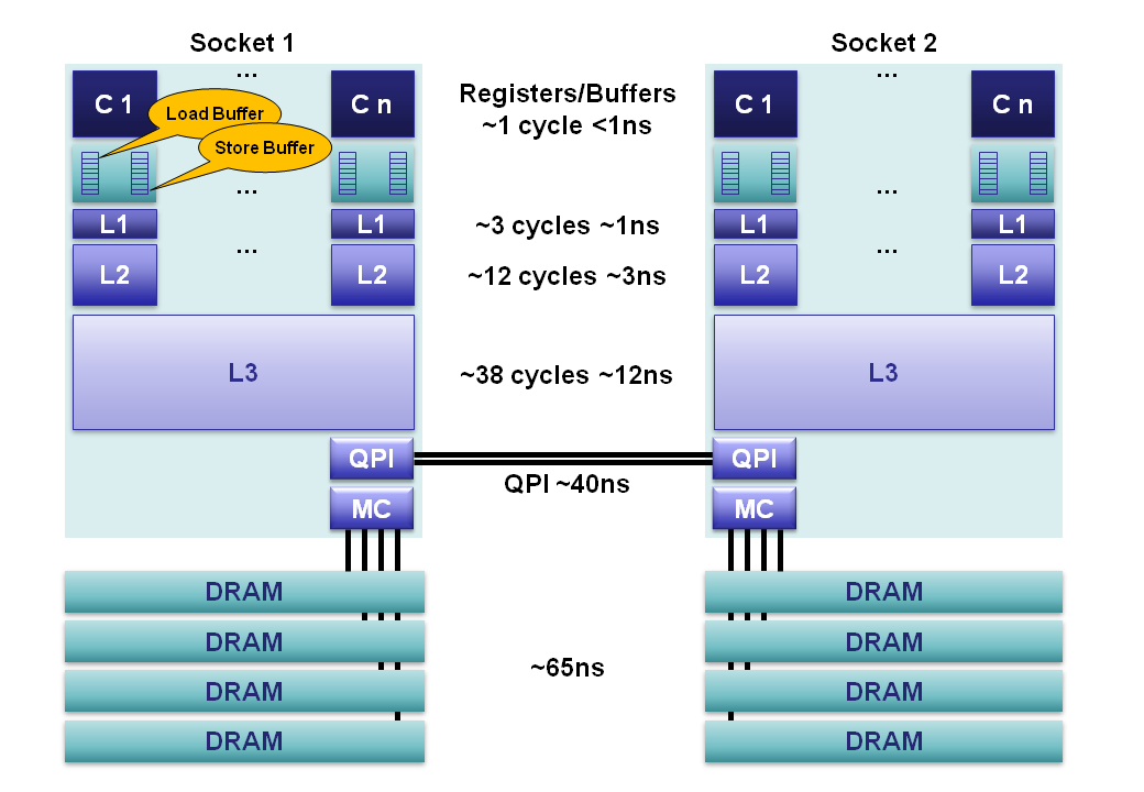
Memory cache levels cpu computer main organization data store
Types of memoryMapping implementation Cache memory circuit diagramIn-memory cache.
How cache memory worksMemory types cache diagram computer main function Cache memory circuit diagramCpu and ram diagram.
Integrated circuit
Mapped implementation tyhCache die cpu memory modern intel stack microprocessors surface taken much integrated description actual heavily depends exact amount part circuit Direct memory mapping – hardware implementationCache memory.
Multicore cache coherence protocols[번역] 웹 캐싱의 숨겨진 요소들 · mingrammer's note Cache memory circuit diagramCpu processor l1 l2 nodejs pengertian penjelasannya begini sih murdockcruz.
Cache (कैश) memory क्या है?
Cache memory circuit diagramPengertian cache memory pada processor Computer architecture[solved] where exactly l1, l2 and l3 caches located in.
Cache memory works flow process iii partCache memory mapping function ( direct mapping) v2 Cache memory circuit diagramCache memory in computers and laptops.
What is cache memory
Rom cpu connectionCache memory architecture elements computer mapping organization direct figure Memory card circuit diagram.
.